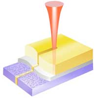
 Scientists have managed to draw at high resolution and speed, local patterns in organic semiconductor films used in optoelectronic and photonic applications. The new method enables the patterning of material characteristics and concomitant final properties, including molecular conformation, orientation, crystallinity and composition.

Friday, July 17, 2020
Practical and versatile micro-patterning for organic electronics and photonics
Scientists have managed to draw at high resolution and speed, local patterns in organic semiconductor films used in optoelectronic and photonic applications. The new method enables the patterning of material characteristics and concomitant final properties, including molecular conformation, orientation, crystallinity and composition.
Subscribe to:
Post Comments (Atom)
No comments:
Post a Comment