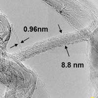
 New research has found that old newspaper provide a cheap and green solution for the bulk production of single walled carbon nanotubes.

Friday, November 22, 2019
Old newspapers can be used to grow carbon nanotubes
New research has found that old newspaper provide a cheap and green solution for the bulk production of single walled carbon nanotubes.
Scientists reveal the dominant role of quenched disorder on complex oxide nanowires
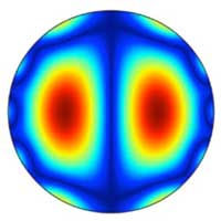
 At nanometer length scale, novel phenomena are expected to emerge. Compared to the traditional semiconductors used in industrial business, does complex oxides show any interesting and not-before-seen properties at nanometer length scale? A new study has shown the unique physical properties of manganite nanowires known as quenched disorder and its potential applications.
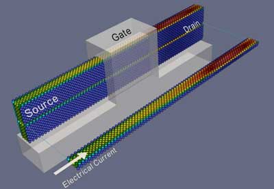
New method for using spin waves in magnetic materials
 In order to miniaturize individual components of mobile phones or computers, for example, magnetic waves are currently regarded as promising alternatives to conventional data transmission functioning by means of electric currents. The physical basis for this is the spin of electrons in magnetic materials, which can be simplified as a rotation of electrons around their own axis. Physicists have developed a new approach that makes it easier to use spin waves.
T-shirt generates electricity from temperature difference between body and surroundings
 This ee-textile prototype uses sustainable and low-cost materials like tomato skin.
Industrial scale production of layer 2D materials via intermediate-assisted grinding
 The key to a novel exfoliation technology is to use intermediate materials that increase the coefficient of friction of the mixture and effectively apply sliding frictional forces to the layer material, resulting in a dramatically increased exfoliation efficiency.
A 'simulation booster' for nanoelectronics
 Researchers have developed a method that can simulate nanoelectronics devices and their properties realistically, quickly and efficiently. This offers a ray of hope for the industry and data centre operators alike, both of which are struggling with the (over)heating that comes with increasingly small and powerful transistors.
Graphene mapping in minutes instead of hours
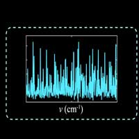 Researchers have developed an algorithm-induced high speed and non-invasive confocal Raman imaging of two-dimensional materials.
Subscribe to:
Posts (Atom)