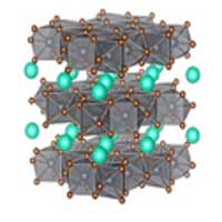
 Researchers have improved on the technique of local processing of composites based on nanoporous glass with addition of silver and copper; now, it is possible to predict with high accuracy the optical properties of a plasmonic component.

Monday, July 13, 2020
A new technique for the production of plasmonics devices
Researchers have improved on the technique of local processing of composites based on nanoporous glass with addition of silver and copper; now, it is possible to predict with high accuracy the optical properties of a plasmonic component.
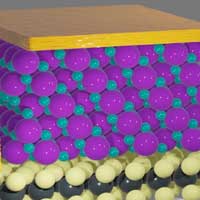
For next-generation semiconductors, 2D tops 3D
 Researchers have developed a memory device using a two-dimensional layered-structure material, unlocking the possibility of commercializing the next-generation memory device that can be stably operated at a low power.
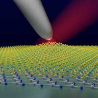
New materials for extra thin computer chips
 For a long time, something important has been regularly neglected in electronics: If you want to make electronic components smaller and smaller, you also need the right insulator materials.
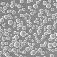
Tiny bubbles make a quantum leap
 Using sophisticated optical microscopy techniques, engineers demonstrate that sufficient strain in 2D material can yield single-photon emitters, key to quantum technologies and future photonic circuitry.
Subscribe to:
Comments (Atom)