 Researchers report infusing contact lenses with gold nanoparticles to create a safer way to see colors.

Wednesday, March 3, 2021
Gold nanocomposite contact lenses that correct color blindness
Researchers report infusing contact lenses with gold nanoparticles to create a safer way to see colors.
The fabrication of photonic wood
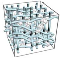 Researchers chemically modified native lignin within wood via a simple, rapid, and scalable UV-assisted photocatalytic oxidation method to fabricate what they call 'photonic wood', which retains a high lignin content of >80%.
Researchers demonstrate highly efficient 3D nano-imaging with XFEL and machine learning
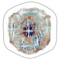 Filming a 3D video of a virus with instantaneous light and AI.
A COSMIC approach to nanoscale science
 The COSMIC Microscopy beamline achieves world-leading resolution of nanomaterials.
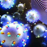
Fluorescent nanodiamonds successfully injected into living cells
 As odd as it sounds, many scientists have attempted to place extremely small diamonds inside living cells. Why? Because nanodiamonds are consistently bright and can give us unique knowledge about the inner life of cells over a long time.
Heat-free optical switch would enable optical quantum computing chips
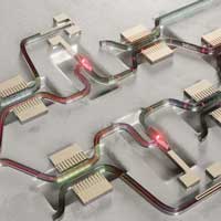 In a potential boost for quantum computing and communication, a European research collaboration reported a new method of controlling and manipulating single photons without generating heat. The solution makes it possible to integrate optical switches and single-photon detectors in a single chip.
Pressure-regulated excitonic feature enhances photocurrent of all-inorganic 2D perovskite
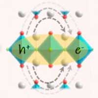 Scientists report significantly enhanced photocurrents in an all-inorganic 2D perovskite, achieving over 3 orders of magnitude increase at the industrially achievable level of 2 GPa in comparison with its initial photocurrent.
Molybdenum disulfide ushers in era of post-silicon photonics
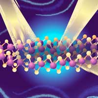 Researchers have measured giant optical anisotropy in layered molybdenum disulfide crystals for the first time. The scientists suggest that such transition metal dichalcogenide crystals could replace silicon in photonics.
'Target identified': teaching a machine how to identify imperfections in 2D materials
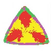 The simple, automated optical identification of fundamentally-different physical areas on these materials could significantly accelerate their application in next-generation, energy-efficient computing, optoelectronics and future smart-phones.
Subscribe to:
Comments (Atom)