Nanopatterning electronic properties of twisted 2D semiconductors
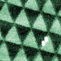
Researchers have demonstrated that atomic lattices of slightly twisted 2D transition metal dichalcogenides undergo extensive lattice reconstruction, which can pattern their optoelectronic properties on nanometre length scale.

 Researchers have demonstrated that atomic lattices of slightly twisted 2D transition metal dichalcogenides undergo extensive lattice reconstruction, which can pattern their optoelectronic properties on nanometre length scale.
No comments:
Post a Comment