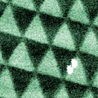
 Researchers have demonstrated that atomic lattices of slightly twisted 2D transition metal dichalcogenides undergo extensive lattice reconstruction, which can pattern their optoelectronic properties on nanometre length scale.

Thursday, May 28, 2020
Nanopatterning electronic properties of twisted 2D semiconductors
Researchers have demonstrated that atomic lattices of slightly twisted 2D transition metal dichalcogenides undergo extensive lattice reconstruction, which can pattern their optoelectronic properties on nanometre length scale.

Photonic crystals: 'even thin is functional'
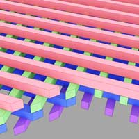 It was always thought that photonic crystals should be thick and bulky to be functional. Scientists now discovered that even very thin 3D photonic band gap crystals are powerful devices to strongly control the flow of light.
Wednesday, May 27, 2020
Kirigami/origami: unfolding the new regime of advanced 3D microfabrication/nanofabrication
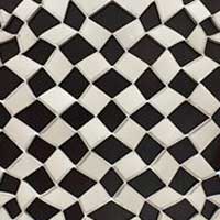 3D micro-/nanofabrication holds the key to build a large variety of micro-/nanoscale materials, structures, devices, and systems with unique properties that do not manifest in their 2D planar counterparts. Recently, scientists have explored some very different 3D fabrication strategies such as kirigami and origami that make use of the science of cutting and folding 2D materials/structures to create versatile 3D shapes.
Construction of hollow nanoreactors for enhanced photo-oxidations
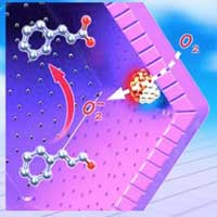 Researchers have demonstrated a facile synthesis of hollow-structured photocatalysts with controllable spatial location of active metals, chemical compositions and tunable shell thickness.
New antiviral and antibacterial nanostructured surface
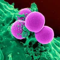 Researchers have found a way to impart durable antiviral and antibacterial properties to an aluminum alloy used in hospitals.
Van der Waals junction spin valves without spacer layer
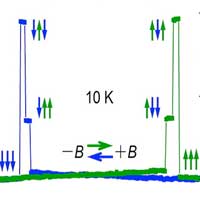 Distinct from traditional spin valves with a sandwich structure consisting of two ferromagnetic metals decoupled by the insertion of a non-magnetic spacer, recently, a research team has demonstrated two-state and three-state spin-valve effects using Fe3GeTe2 vdW homo-junctions without any spacer layer. Realization of multi spin states using the vdW interfaces could be important for non-volatile spintronic applications.
Using in-situ AFM to get a sneak peek of a key process in battery 'life'
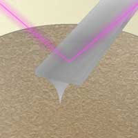 Researchers visualized the formation of a solid electrolyte interphase on battery-grade carbonaceous electrode materials using in situ atomic force microscopy (AFM). This will help researchers design and build batteries with higher performance and durability.
Subscribe to:
Posts (Atom)