 Using a technique called molecular layer etching can help manufacturers and researchers develop new ways of making nanostructures.
Wednesday, February 12, 2020
New etching technique could advance the way semiconductor devices are made
 Using a technique called molecular layer etching can help manufacturers and researchers develop new ways of making nanostructures.
Graphene forms under microscope's eye (w/video)
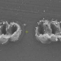 You don't need a big laser to make laser-induced graphene. Scientists are using a very small visible beam to burn the foamy form of carbon into microscopic patterns.
Bubble-capturing surface helps get rid of foam
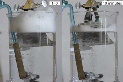 Bubbly buildup can hinder many industrial processes, but a new method can reduce or even eliminate it.
Discovery brings nanoscale thermal switches needed for next-gen computing
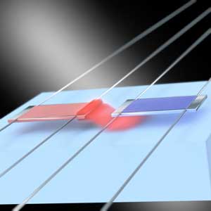 Researchers have developed nanoscale thermal switches that are key to thermal management of nanoscale devices, refrigeration, data storage, thermal computing and heat management of buildings.
X-ray microscopy shows that nanoparticles can change cells
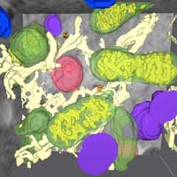 Nanoparticles easily enter into cells. New insights about how they are distributed and what they do there are shown for the first time by high-resolution 3D microscopy images.
Wearable medical sensors to get major sensitivity boost
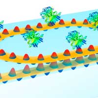 Scientists describe a way to increase the sensitivity of biological detectors to the point where they can be used in mobile and wearable devices.
Small world: atom-scale materials are the next tech frontier
 'Atomaterials' is short for 'atomic materials', so called because their properties depend on the precise configuration of their atoms.
Something from nothing: Using waste heat to power electronics
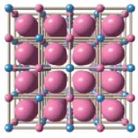 Researchers develop an improved energy-harvesting device that can convert heat to electricity.
Subscribe to:
Comments (Atom)
