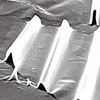
 Strain engineering can significantly manipulate the two-dimensional (2D) materials' electronic and optical properties, which endow it the potential applications in optoelectronics and nanophotonics.

Monday, November 23, 2020
Strain engineering of 2D semiconductors and graphene
Strain engineering can significantly manipulate the two-dimensional (2D) materials' electronic and optical properties, which endow it the potential applications in optoelectronics and nanophotonics.

Researchers find conformational disorder tuning charge carrier mobility in 2D perovskites
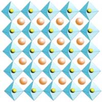 Researchers have synthesized a series of 2D organic-inorganic hybrid perovskites films with large organic spacer cations, and found that mobility and broadband emission showed strong dependence on the molecular conformational order of organic cations.
Contact lenses for diagnostic and therapeutic use
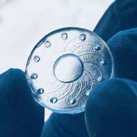 Specially engineered contact lenses use tears to monitor patient health.
Perfect imperfection: Electrode defects boost resistive memory efficiency
 Researchers have studied the impact of electrode surface morphology on the properties of a resistive switching memory cell. It turned out that thicker electrodes have greater surface roughness and are associated with markedly better memory cell characteristics.
Controlling fully integrated nanodiamonds
 Physicists have succeeded in fully integrating nanodiamonds into nanophotonic circuits and at the same time addressing several of these nanodiamonds optically. The study creates the basis for future applications in the field of quantum sensing schemes or quantum information processors.
Unlocking cheaper, sustainable chemicals
 A new technique to make cheaper more efficient biological enzyme hybrids could have valuable applications in future water recycling, targeted drug manufacturing and other industries.
Saturday, November 21, 2020
From lab to industry? Ideally ordered porous titania films, made at scale
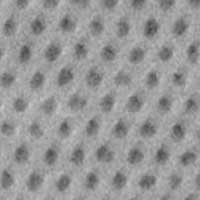 Researchers have realized high-throughput production of thin, ordered through-hole membranes of titanium dioxide.
Subscribe to:
Posts (Atom)