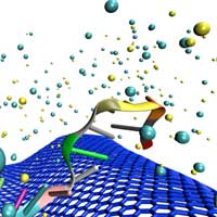
 Crumpling graphene makes it more than ten thousand times more sensitive to DNA by creating electrical 'hot spots'.

Tuesday, March 24, 2020
Crumpled graphene makes ultra-sensitive cancer DNA detector
Crumpling graphene makes it more than ten thousand times more sensitive to DNA by creating electrical 'hot spots'.

Monday, March 23, 2020
Novel metal-organic framework is potential next-gen semiconductor
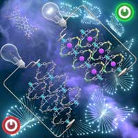 Researchers demonstrated a novel double-helical metal organic framework architecture in a partially oxidized form that conducts electricity, potentially making it a next-generation semiconductor.
A key development in the drive for energy-efficient electronics
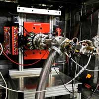 Scientists have made a breakthrough in the development of a new generation of electronics that will require less power and generate less heat. It involves exploiting the complex quantum properties of electrons - in this case, the spin state of electrons.
Unraveling the optical parameters: New method to optimize plasmon enhanced spectroscopy
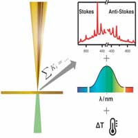 Researchers report the first accessible method to gain unprecedented insights into the plasmonic activity of a single nanoparticle during a typical tip-enhanced Raman spectroscopy experiment.
New metasurface helps make the switch to terahertz frequencies
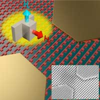 The new highly efficient metasurface switch needs no metal or backing material. This means detectors using the switch would be smaller, thinner, more efficient, and require less power.
Engineered nanowrappers carry and release tiny cargo
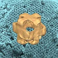 Scientists have discovered a new method for creating hollow metallic nanostructures with regularly spaced and sized pores. The pores are large and regular enough to carry molecule or nanoscale-size particles of drugs and other substances.
Wrapped, layered semiconductors catch the light
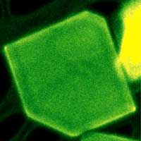 Researchers discovered a new way to integrate semiconductor layers to make heterostructures. They found that layers of different compounds of tin and sulfur spontaneously separated during synthesis. This unique structure translates into excellent light absorption and energy transfer properties.
Subscribe to:
Posts (Atom)