 Researchers replaced widely-used, but environmentally unfriendly, R134a refrigerant with the more energy-efficient R600a. They dosed R600a with multi-walled carbon nanotubes.
Saturday, May 30, 2020
Carbon nanotubes can make home refrigeration more accessible for low-income households
 Researchers replaced widely-used, but environmentally unfriendly, R134a refrigerant with the more energy-efficient R600a. They dosed R600a with multi-walled carbon nanotubes.
New stretchable, self-healing and illuminating electronic material for wearables and soft robots
 Imagine a flexible digital screen that heals itself when it cracks, or a light-emitting robot that locates survivors in dark, dangerous environments or carries out farming and space exploration tasks. A novel material could turn these ideas into reality.
Friday, May 29, 2020
Paper-thin gallium oxide transistor handles more than 8,000 volts
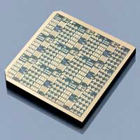 The advancement surpasses silicon and other mature technologies, and could help improve distances that electric cars, locomotives can travel.
Researchers develop experimental rapid COVID-19 test using nanoparticle technique
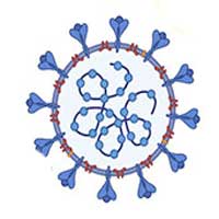 Advanced nanotechnology provides 'naked eye' visual detection of virus in 10 minutes.
Thursday, May 28, 2020
Nanopatterning electronic properties of twisted 2D semiconductors
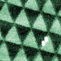 Researchers have demonstrated that atomic lattices of slightly twisted 2D transition metal dichalcogenides undergo extensive lattice reconstruction, which can pattern their optoelectronic properties on nanometre length scale.
Photonic crystals: 'even thin is functional'
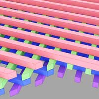 It was always thought that photonic crystals should be thick and bulky to be functional. Scientists now discovered that even very thin 3D photonic band gap crystals are powerful devices to strongly control the flow of light.
Wednesday, May 27, 2020
Kirigami/origami: unfolding the new regime of advanced 3D microfabrication/nanofabrication
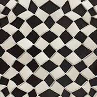 3D micro-/nanofabrication holds the key to build a large variety of micro-/nanoscale materials, structures, devices, and systems with unique properties that do not manifest in their 2D planar counterparts. Recently, scientists have explored some very different 3D fabrication strategies such as kirigami and origami that make use of the science of cutting and folding 2D materials/structures to create versatile 3D shapes.
Construction of hollow nanoreactors for enhanced photo-oxidations
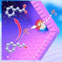 Researchers have demonstrated a facile synthesis of hollow-structured photocatalysts with controllable spatial location of active metals, chemical compositions and tunable shell thickness.
New antiviral and antibacterial nanostructured surface
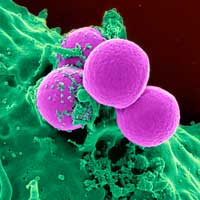 Researchers have found a way to impart durable antiviral and antibacterial properties to an aluminum alloy used in hospitals.
Van der Waals junction spin valves without spacer layer
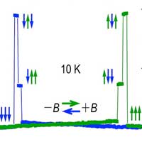 Distinct from traditional spin valves with a sandwich structure consisting of two ferromagnetic metals decoupled by the insertion of a non-magnetic spacer, recently, a research team has demonstrated two-state and three-state spin-valve effects using Fe3GeTe2 vdW homo-junctions without any spacer layer. Realization of multi spin states using the vdW interfaces could be important for non-volatile spintronic applications.
Using in-situ AFM to get a sneak peek of a key process in battery 'life'
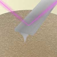 Researchers visualized the formation of a solid electrolyte interphase on battery-grade carbonaceous electrode materials using in situ atomic force microscopy (AFM). This will help researchers design and build batteries with higher performance and durability.
Scientists devise a way to determine the viability of predicted 2D materials
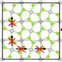 An international team of researchers has proposed a new way to test the structural stability of predicted 2D materials. The testing revealed a number of materials erroneously proposed earlier. The scholars believe that the use of the new method will further help to avoid mistakes in the development of two-dimensional nanomaterials that are in high demand in the modern world.
Self-cleaning aluminium surface without scrubbing and using chemicals
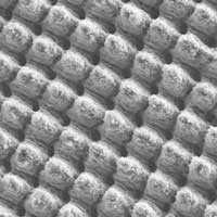 Scientists have developed a self-cleaning metallic surface that is structured with a laser process in such a way that water droplets no longer adhere and dirt particles can be removed from the surface.
Tuesday, May 26, 2020
Flow-through electrodes make hydrogen 50 times faster
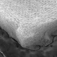 Experiments find the sweet spot for surface area and bubbles to store energy.
Nanodevices show how cells change with time, by tracking from the inside (w/video)
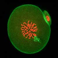 For the first time, scientists have added microscopic tracking devices into the interior of cells, giving a peek into how development starts.
Untwisting plastics for charging Internet-of-things devices
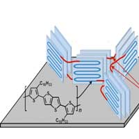 Scientists are unraveling the properties of electricity-conducting plastics so they can be used in future energy-harvesting devices.
The negative-capacitance transistor - Building an ideal MOSFET
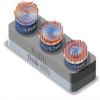 Electrical and computer engineering researchers demystify the role of negative capacitance in modern MOSFETs.
Lossless conduction at the edges
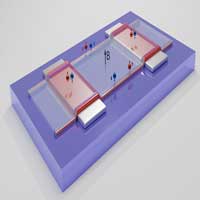 Atomically thin layers of the semimetal tungsten ditelluride conduct electricity losslessly along narrow, one-dimensional channels at the crystal edges. The material is therefore a second-order topological insulator.
Novel insight reveals topological tangle in unexpected corner of the universe
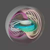 Scientists find a unique knotted structure - one that repeats itself throughout nature - in a ferroelectric nanoparticle, a material with promising applications in microelectronics and computing.
New single particle diffraction method
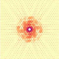 Algorithms, gold and holographic references boost biomolecule diffraction.
Study finds electrical fields can throw a curveball
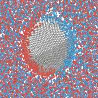 Particle-scale phenomenon akin to the swerving of a curveball could allow selective separation of suspended nanomaterials.
Nanoneedles to increase the capacity and robustness of digital memories
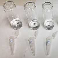 Researchers developed a new technique to locally modify the properties of a metamagnetic material. The method consists in applying local pressure to the surface of the material using nanometric needles and allows a much more easy and local modification than current methods.
High-Security identification that cannot be counterfeited
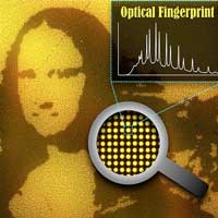 Reseaerchers create millimeter-size chips with unique color patterns that cannot be forged.
Monday, May 25, 2020
Understanding ceramic materials' 'mortar' may reveal ways to improve them
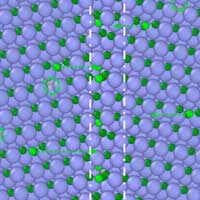 New research shows that in the important ceramic material silicon carbide, carbon atoms collect at those grain boundaries when the material is exposed to radiation. The finding could help engineers better understand the properties of ceramics and could aid in fine-tuning a new generation of ceramic materials.
New double-contrast technique picks up small tumors on MRI
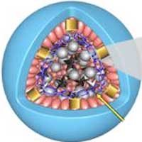 A new technique offers a significant advance in using magnetic resonance imaging to pick out even very small tumors from normal tissue.
Researchers obtain 2D magnetism in both carbon and polyradical nanosheets
 Scientists report that they have obtained edge-induced room-temperature ferromagnetism in both carbon nanosheets and two-dimension (2D) organic antiferromagnetic polyradical nanosheets.
Watching single protons moving at water-solid interfaces
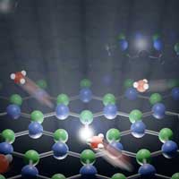 A new study has provided the first-ever glimpse of the behavior of protons when water comes into contact with a solid surface, going down to the ultimate scale of single proton and single charge.
New molecules for innovative high-tech materials
 Sandwich compounds based on rare earths might serve as novel molecular materials for more efficient storage media or displays in future.
Microbial cyborgs: Bacteria supplying power
 One day, 'microbial cyborgs' might be used in fuel cells, biosensors, or bioreactors. Scientists have created the necessary prerequisite by developing a programmable, biohybrid system consisting of a nanocomposite and the Shewanella oneidensis bacterium that produces electrons.
Record-high data transmission using a soliton crystal
 An international team of researchers has developed an efficient way to create micro-combs and exploit them in highly performing and robust frequency multiplexed optical fibre networks.
Friday, May 22, 2020
Oriented hexagonal boron nitride foster new type of information carrier
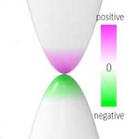 A novel alternative to current computers is to utilize the wave quantum number of the electrons by which the information encoding is possible without physically moving the carriers. This study shows that manipulation of the wave quantum number is possible by controlling the stacking configuration and the orientation of different two-dimensional materials.
3D-printing functional bone tissues with nanoengineered bioink
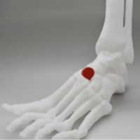 A novel printable bioink could be used to create anatomical-scale functional tissues.
Thursday, May 21, 2020
'One-way' electronic devices enter the mainstream
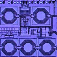 Engineers build high-performance non-reciprocal devices on a compact chip, paving the way for applications from two-way wireless to quantum computing.
Implantable biosensor operates without batteries
 Researchers have revealed their new biodegradable motion sensor - paving the way for implanted nanotechnology that could help future sports professionals better monitor their movements to aid rapid improvements, or help caregivers remotely monitor people living with dementia.
Researchers report new method for characterizing materials that might eventually help store energy
 As the search for materials to efficiently address energy storage and transport needs continues, researchers report new techniques for characterizing complex materials with the potential to overcome these challenges.
Membrane nanopore transport gets picky
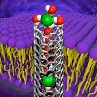 Trying to determine how negatively charged ions squeeze through a carbon nanotube 20,000 times smaller than a human hair is no easy feat. Not only did scientists do that but they found that those ions are unexpectedly picky depending on the anion.
Ultrasonic technique discloses the identity of elastic constant of graphite crystal
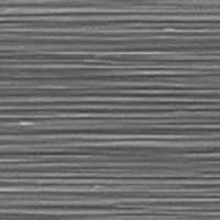 Scientists evaluated the interplanar bond strength of graphene by measuring the elastic constant of graphite, demonstrating that the elastic constant of monocrystalline graphite was above 45 gigapascal, which was higher than conventionally believed.
Novel device harnesses shadows to generate electricity
 Researchers are giving shadows a positive spin by demonstrating a way to harness this common but often overlooked optical effect to generate electricity. This novel concept opens up new approaches in generating green energy under indoor lighting conditions to power electronics.
Novel nanostructure stimulates growth of stem cells for Parkinson's disease treatment
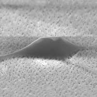 Researchers have invented a nanostructure that can stimulate neural stem cells to differentiate into nerve cells. They found that the transplantation of these nerve cells into rats with Parkinson's disease progressively improved their symptoms, with the new cells replacing damaged nerve cells around the transplantation site.
Wednesday, May 20, 2020
Synthesizing large-scale 2D conjugated polymers
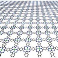 Structurally reconfigurable two-dimensional conjugated polymers can give a new breadth to applications of two-dimensional materials in electronics.
Breakthrough in research on production of 2D crystals with excellent optical properties
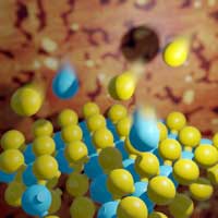 For the first time, monolayers of transition metal dichalcogenides with excellent optical properties were grown.
Researchers develop material capable of being invisible or reflective in IR spectrum
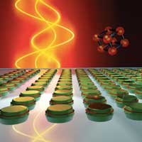 Researchers have proposed a new metamaterial capable of changing its optical properties without any mechanical input. This development could result in a significant improvement in the reliability of complex optical devices while making them cheaper to manufacture.
Visualizing at the single-molecule level the processes involved in a biological nanomachine
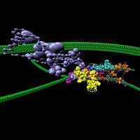 Researchers have for the first time ever succeeded in visualizing at the single-molecule level the processes involved in a biological nanomachine, known as the cellulosome, as it degrades crystalline cellulose. The fundamental insights thus obtained could support sustainable concepts of cellulose utilization to make a breakthrough in industrial biotechnology.
'Nanometrology lab on a chip' within reach thanks to new compact, optical sensor
 Researchers have developed a new, integrated optical sensor that provides increased resolution in measurements and paves the way for fully integrated and compact optical sensors including lasers and detectors for on-chip sensing platforms.
Attosecond physics: Quantum brakes in molecules
 Physicists measured the flight times of electrons emitted from a specific atom in a molecule upon excitation with laser light. This has enabled them to measure the influence of the molecule itself on the kinetics of emission.
Nanobowls serve up chemotherapy drugs to cancer cells
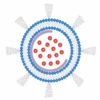 Researchers report a way to stabilize liposomes by embedding a stiff nanobowl in their inner cavity.
One-step synthesis of new nanomaterials with higher anti-SARS-CoV-2 activity
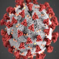 The goal of a new project is to use green, environmentally friendly, one-step synthesis routes of new silver-nanoparticle-based nanomaterials with anti-SARS-CoV-2 activity.
Scientists use light to accelerate supercurrents, access forbidden light, quantum world
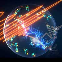 Scientists are using light waves to accelerate supercurrents and access the unique properties of the quantum world, including forbidden light emissions that one day could be applied to high-speed, quantum computers, communications and other technologies.
Tuesday, May 19, 2020
True colors: Using X-rays to trace the evolution of insects' structural colors
 While different families of insects grow different kinds of nanostructures, they all converge on similar lustrous qualities. These are not colors made with pigments, so they don't fade with time. The crystalline structures reflect light in such a way that the colors are iridescent, brighter and more arresting than the colors we can produce chemically.
Subscribe to:
Posts (Atom)

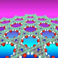 Making 2D topological polymers a reality.